You need a DC generator source, but for some reason, can’t purchase one? You can build your linear source, in this post is shown how.
Design
A DC linear source converts AC voltage from the home outlet to DC to supply circuits and electronic components. Next is the block diagram.

Transformer
This component’s operation is explained in a post, whose link is below.
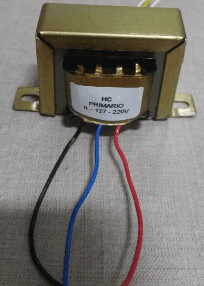
A transformer reduces outlet voltage. The primary winding has wires in black (ground), red (220 V), and blue (127 V) colors.
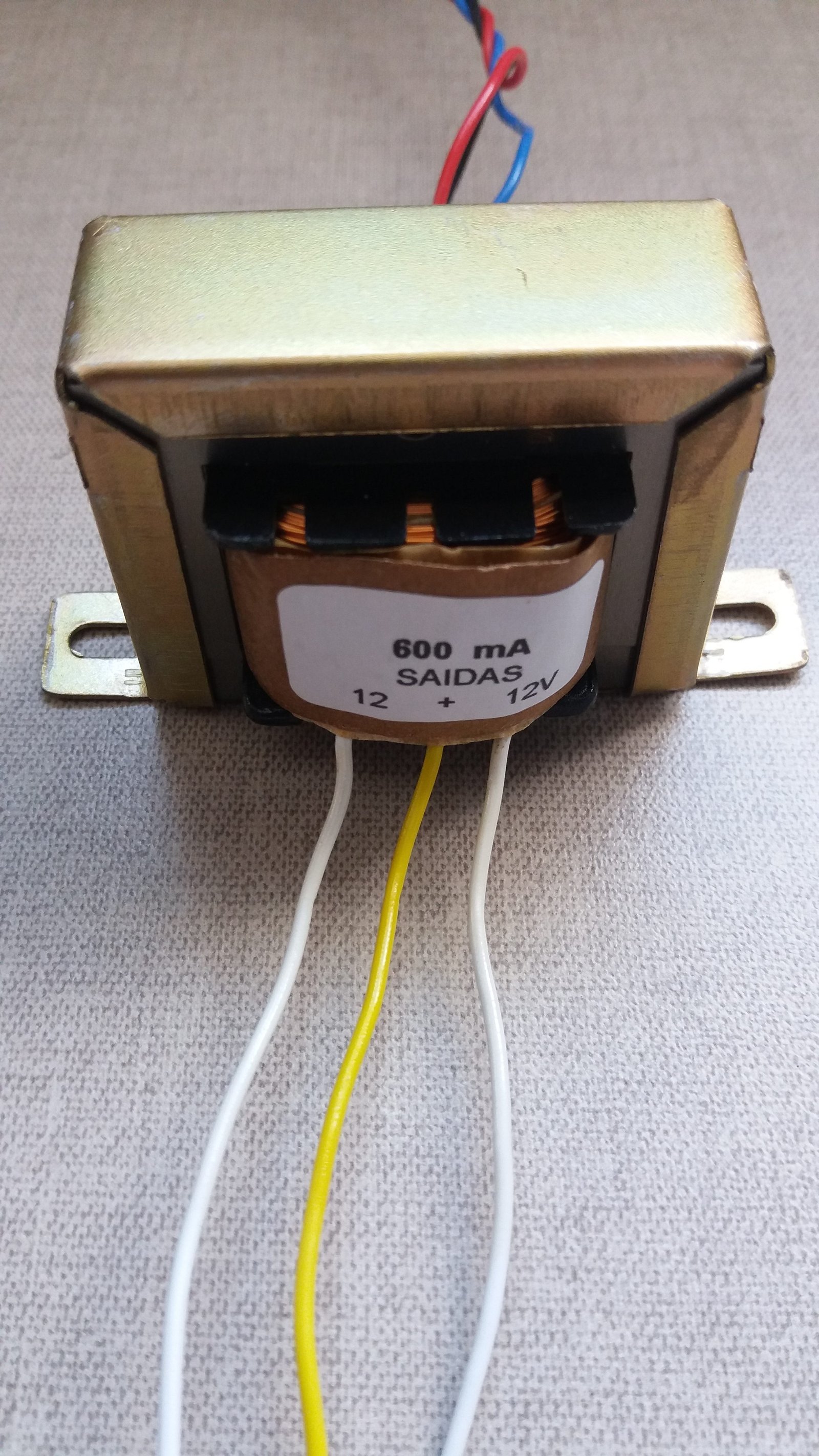
The secondary winding has white wires linked to phases and a yellow one as neutral.
Rectifier
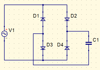
The rectifier is a full wave diode bridge.
Diodes are all 1N4007, currently the most common for this application. The operation of diodes and bridges has already been shown in a dedicated post.
Filter
The signal in output of rectifying bridge is pulsed continuously. Source’s output must be a straight continuous signal as stable as possible. First, must be put a capacitor in diode bridge’s output.
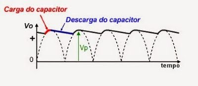
During maximum amplitude of a pulsed continuous signal, the capacitor is charged (red in figure below). When signal loses amplitude, capacitor discharges (blue). But soon charges up again, the output signal is a DC voltage with ripple.
Ripple factor in % is calculated in this form. V_{RMS} is voltage in RMS of waveform and V_{DC} is output`s value.
r=\frac{V_{RMS}}{V_{DC}}\cdot 100
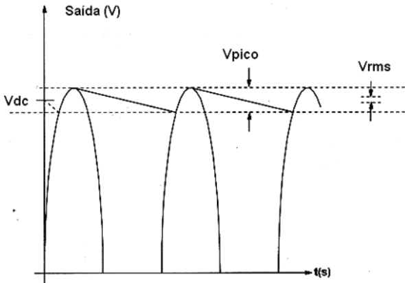
It is recommended that ripple factor be at most 10%. Which value must be the capacitor? Transformer has secondary 12+12 V, therefore peak voltage V_{p} is:
V_{p}=\sqrt{2}\cdot (12+12)=\sqrt{2}\cdot 24=33,94 V
Considering voltage drop in both diodes.
V_{p}=33,54-1,4=32,54V
If ripple is 10%, then voltage variation \Delta V is 3.25 V, because it is 10% of peak voltage. To design the capacitor value, must use this formula.
\Delta V=\frac{I}{fC}
f is frequency, which is 60 Hz. To calculate I, must define the load resistor in parallel with capacitor.
I put a red LED in series with R1, value of the latter is arbitrary, therefore current I is:
I=\frac{V_{C}-V_{LED}}{R1}
I=\frac{32.54-2}{1000}=30.54mA
Using previous equation.
3.25=\frac{30.54m}{60\cdot C}
C=\frac{30.54m}{195}=0.1566m=156.6\mu F
This is the minimum value of electrolytic capacitor, there is no problem to use higher values, because higher means that will take longer to discharge. I choose 470 μF because is minimum commercial value I have. Capacitor voltage must be bigger than peak voltage, or it will burn. Therefore C1 is 470 μF x 50 V.
Regulator
The voltage output of linear source until now is 16 V, with small instability for more or less.
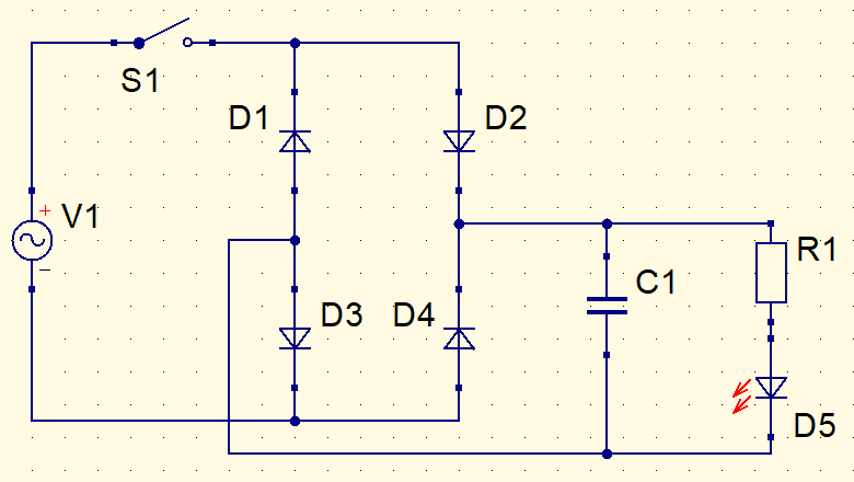
Output voltage must be stable and controllable. What to do? Was used the integrated circuit LM317T, whose datasheet can be found in this link. Datasheet already shows a voltage regulator circuit.
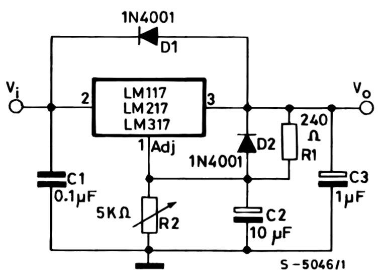
C1 capacitor does signal decoupling, used when regulator is far from source. A transient signal, coming from AC fluctuations, pass through this capacitor and is grounded, improving signal quality. This feature is called ripple rejection. In this project, regulator is close to source, so there is no need for C1. C2 has the same function. C3 is to improve transient response in output signal.
For what serve D1 and D2 diodes? When C2 and C3 unload, discharge current goes to diodes, protecting LM317T. Because when capacitors unload, they liberate a reverse current for a short time period. The chosen types are 1N4007.
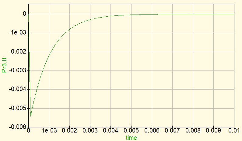
Resistor R1 and potentiometer R2 determine voltage band of regulator. In datasheet we can see the equation of circuit’s output voltage Vo.
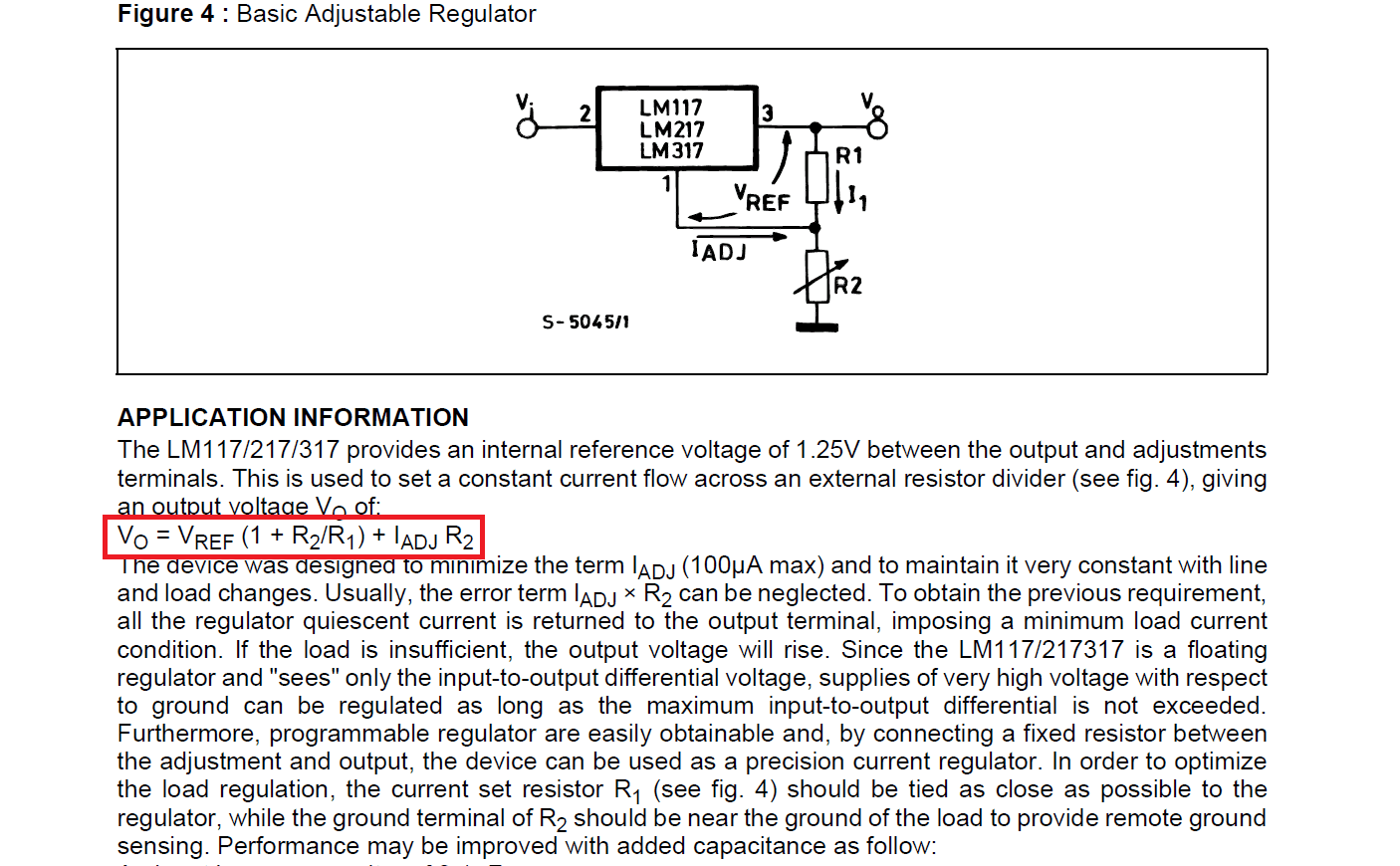
The values of I_{ADJ} and V_{REF} also are shown.
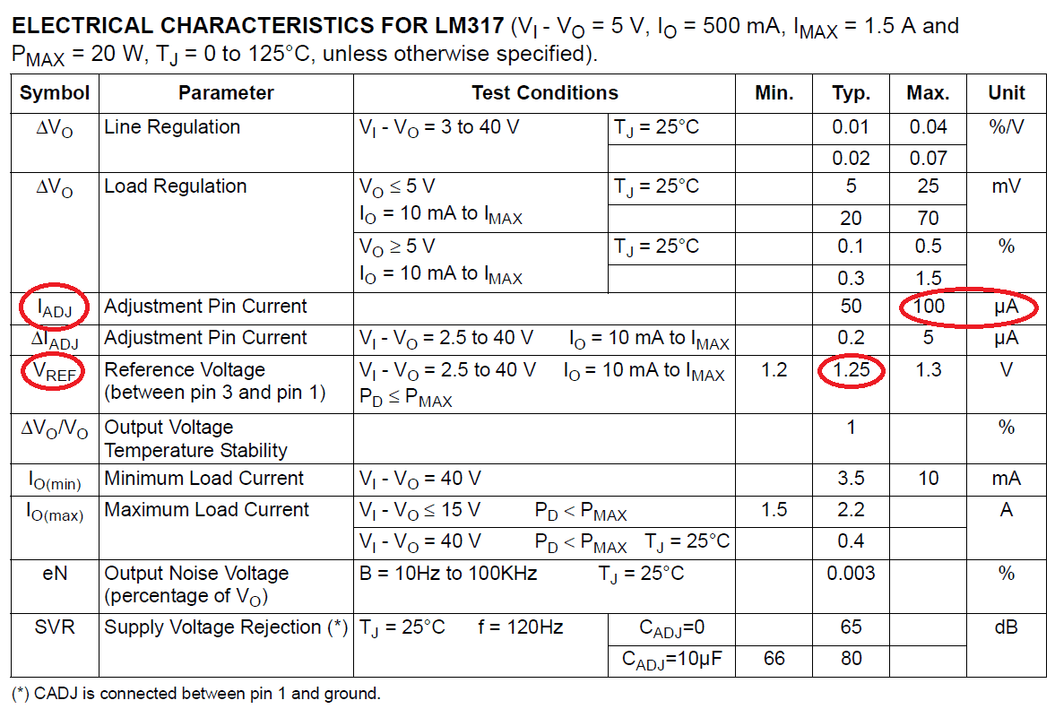
Value of R2 potentiometer is 10 kΩ, which was arbitrarily chosen. Calculating R1 with output voltage as 15 V.
Vo=V_{REF}\cdot \left ( 1+\frac{R2}{R1} \right )+R2\cdot I_{ADJ}
15=1,25\cdot \left ( 1+\frac{10k}{R1} \right )+10k\cdot 100\mu
R1=0,98k\Omega
Must adopt the commercial value of 1 kΩ.
Assembling and test
Finally, the part to assemble a DC linear source. This is a connection diagram of LM317T’s terminals.

Complete schematic of the linear source.

You can assemble in a printed circuit board or terminal bridge. I picked a terminal bridge because assemble is faster and circuit size isn’t so important.

The complete circuit in a bridge.
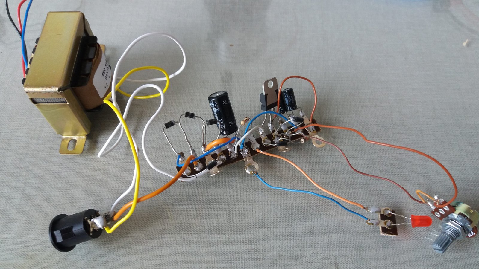
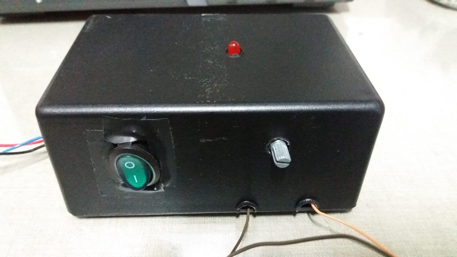
The circuit has been put inside a box, whose dimensions are: 12.5 cm in length; 8.5 cm in width, and 5.5 cm height.
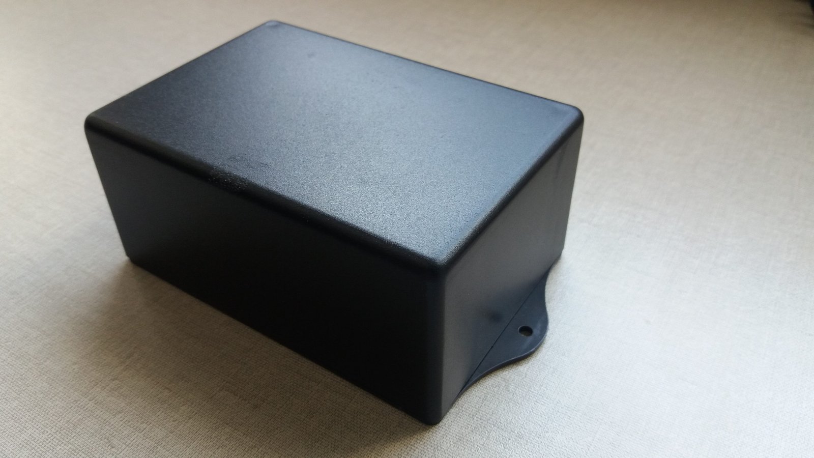
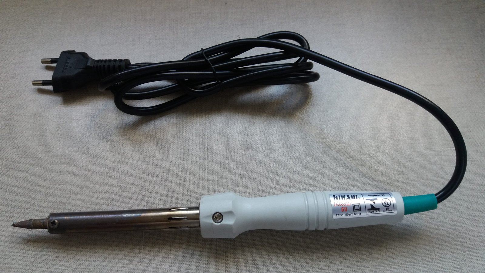
Was needed to make holes in the box for power button, potentiometer, LED, and output terminals to stay outside. An option is to use a 50 W soldering iron to make holes.
The linear source is ready. Must provide voltages between 1.36 V and 14.5 V, these values can vary a bit due to the resistor’s tolerance.


I’m always learning more blog wonder i liked thank you for your help.
Your website is amazing congratulations, visit mine too:
https://strelato.com
.