MEMS manufacturing is similar to process used to fabricate microelectronic circuits. The bulk micromachining is today’s subject.
In case you don’t know what MEMS are, it is recommendable to read the post which link is below.
Bulk micromachining
This is a subtractive method, are removed parts of silicon substrate in front or back side to obtain desired shape. The first stage is put a thin silicon oxide (SiO_{2}) layer in substrate.
![]()
Exist two methods to put a SiO_{2} layer: dry or wet oxidation. In dry oxidation, substrate is placed in a heater with quartz tube, which temperature is between 900°C (1652ºF) and 1200°C (2192ºF) and it’s in contact with oxygen to form the following chemical reaction.
Si+O_{2}\rightarrow SiO_{2}

In wet oxidation, substrate receives a steam at 95ºC (203ºF) with oxygen bubbles, producing the chemical reaction below. The substrate is submitted to a temperature between 800ºC (1472ºF) and 1000ºC (1832ºF).
Si+2H_{2}O\rightarrow SiO_{2}+2H_{2}

In wet oxidation, layer grows faster than in dry and it’s used to thicker layers. Dry oxidation is slower and for thinner layers. Video below shows an animation of SiO_{2} layer formation in wet and dry processes, oxygen atoms are represented by red particles.
Part of SiO_{2} must be removed. This is done through photolithography, consist in put a photoresist layer and then a mask. An ultraviolet light chemically changes the part non-protected by mask to be removed. More details about photolithography will be explained in a post about manufacturing of integrated circuits or chips.
 Then, comes etching to remove part of silicon substrate.
Wet etching process
Like in oxidation, there are wet and dry procedures to remove part of silicon. In wet, material is immersed in an aqueous solution, which solvent is water, to partial etching. The solute is potassium hydroxide (KOH), hydrofluoric acid (HF), TMAH (N(CH_{3})_{4}^{+}OH^{-}) or a mixture of hydrofluoric, nitric and acetic (HNA).
Dry etching process
In dry process, it’s used vapor or reactive ions from a low pressure plasma. The material is inside a vacuum chamber, with electrodes supplied by a RF power source with frequency in kilohertz (kHz) or Megahertz (MHz). A gas is injected in chamber and becomes a plasma, electric field between electrodes attracts ions and electrons to substrate, making a physical and chemical removal.

Other etching alternative is use xenon difluoride vapor (XeF_{2}), making the following chemical reaction with silicon.
2XeF_{2}+Si\rightarrow 2Xe+SiF_{4}
Wet process is cheaper than the dry one. However, dry process is more accurate and use less chemical products. In addition to this, wet method can contaminate water with toxic products.
Isotropic and anisotropic etching
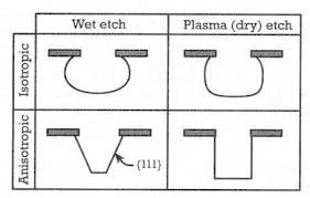
Etching in substrate can be two types: Isotropic, where corrosion rate is equal in all directions, and anisotropic, corrosion rate is higher in one direction.

Other factors which influence in formation of cross section and corrosion rate:
- Silicon’s crystalline structure.
- Temperature.
- Used substance for removal.
- Silicon doping.


