
The junction field effect transistor (FET) is a component with many applications. In this post, are shown the structure and the operation.
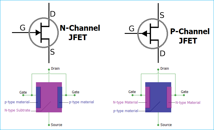
Internal structure of junction field effect transistor
Consists in a substrate of semiconductor material, usually silicon, doped to have lack or excess of electrons. In JFET, part of semiconductor connected to gate is doped with opposite type of the substrate. Field effect transistor terminals are: gate, drain and source. Type N materials are doped to have more electrons and the P type, to have less electrons.
Operation
The field effect transistor is also called unipolar, because its use only electrons or holes (empty spaces without electrons, therefore, positive charges) for current circulation inside the device. While the bipolar junction transistor (BJT) uses both. On JFET, current flows only through substrate and it’s controlled by voltage on gate terminal. On p-n junctions, there is a depletion region, as on diode’s p-n junction.
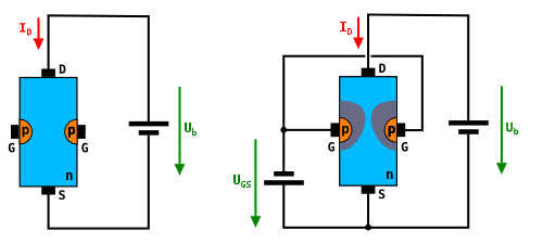
If you put a direct voltage between gate and source, the transistor can burn. To understand what depletion region expands, access the post about diode operation.
Characteristic curves and equations
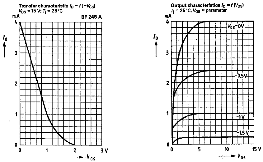
The Shockley equation relates drain current (I_{D}), that passes through drain and source terminals, with gate-source voltage (V_{GS}).
I_{D}=I_{DSS}(1-\frac{V_{GS}}{V_{p}})^2
Where I_{DSS} is the maximum drain current when V_{GS}=0 and V_{DS} is higher than pinch-off voltage (V_{p}), which is the voltage that separates the ohmic or linear region, where there is I_{D} variation, from saturation region. For example, when V_{GS}=0, V_{p} of BF245 transistor is 7 V. On ohmic region, JFET can be used as voltage controlled resistor. This is the equation of transistor resistance between drain and source.
r_{d}=\frac{r_{o}}{(1-V_{GS}/V_{p})^2}
- r_{o} is the resistance when V_{GS}=0.
- r_{d} is the resistance when V_{GS}<0.
The next post will be about another type of field effect transistor, the MOSFET.

 is a component with many applications. In this post, are shown the structure and the operation.)