
The post’s subject is class B and class AB amplifiers, including operation, a project and comparison with the class A.
Class A amplifier
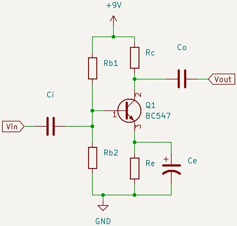
The class A amplifier is nothing more than a common emitter. It has a conduction angle of 360º, by that, the transistor is always on, even when is no input signal. Therefore, output signal has the same shape of input signal, but its amplified. However, due to this feature, the maximum efficiency is only 25%, with a transformer, it can reach 50%.
Class B amplifier
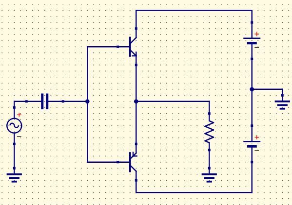
Two transistors, a NPN and a PNP form a push-pull configuration, where a transistor only conduct on one wave’s half, in other words, it has a conduction angle of 180º. NPN conducts when signal is positive and PNP conducts when wave’s amplitude is negative. Without AC on input, both transistors are in cut. This is the reason for high efficiency, class B amplifier can obtain a maximum efficiency of 78.5%.
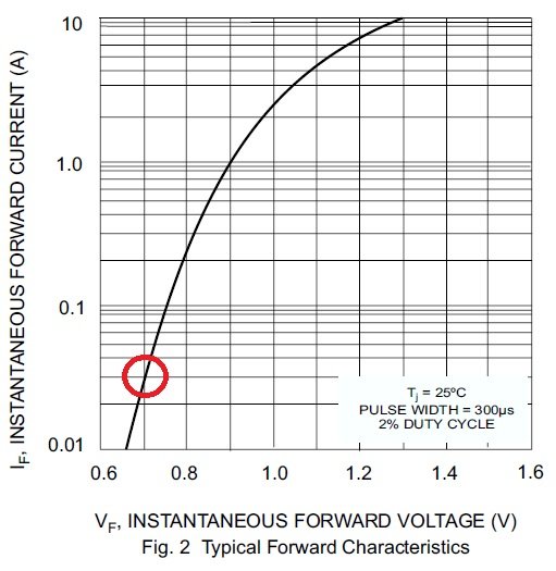
The class B amplifier’s disadvantage is the distortion in output, also known as crossover distortion. When the input signal’s amplitude is close to zero, both transistors are on cutoff region, therefore, don’t conduct. For the transistor to leave the cut mode, voltage on base must be higher than base-emitter voltage (V_{BE}). In most of BJT transistors, you can consider V_{BE} as 0.7V and -0.7V, for NPN and PNP, respectively.
Class AB amplifier
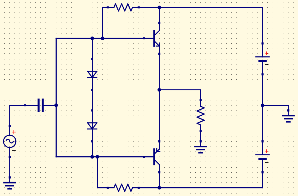
This circuit corrects class B’s crossover distortion, polarizing transistors so that they continuing conducting, even when voltage input is close to zero. Since voltages between base and emitter V_{BE} of NPN and PNP are approximately 0.7V and -0.7V, respectively, the diodes are positioned so that the voltage between the bases is 1.4V. While the resistors’ role is to create a bias current, to adjust bases’ voltages.
Class AB’s efficiency is between 50% and 60%, a little lower than class B, due to transistors biasing. However, its still much higher than the class A.
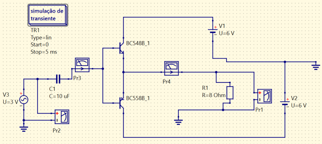
Designing a class AB amplifier
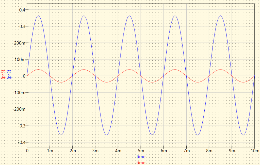
Voltage supply V_{CC} is 6V, a value arbitrarily chosen. Diodes are 1N4007 and NPN and PNP transistors are BC548B and BC558B, respectively. To calculate the resistors, its necessary to determine bias current I_{BIAS}, represented by the red arrow on the figure below.
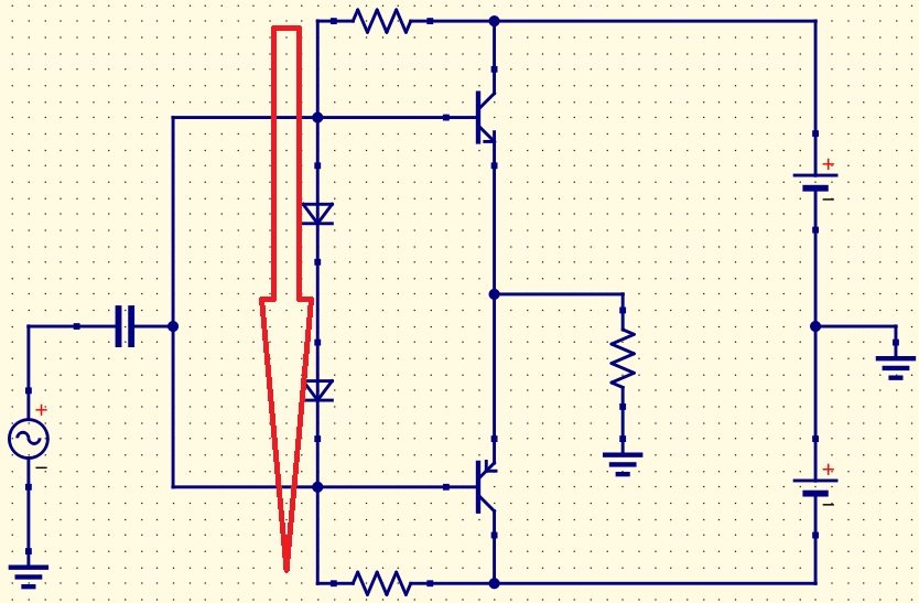
The formula to calculate resistor R.
I_{BIAS}=\frac{V_{CC}-2\cdot V_{BE}+V_{CC}}{2R}
30m=\frac{6-2\cdot 0.7+6}{2\cdot R}
R=175.1\Omega
R commercial value can be 150Ω or 180Ω.
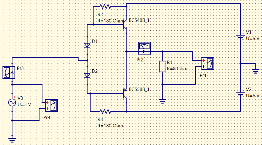
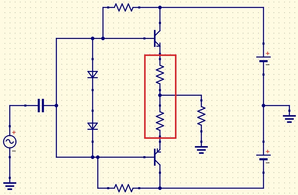
It may be necessary to use resistors R_{E} connected to the emitter terminals. These resistors must be between 0.47Ω and 10Ω. To calculate the exact value, just divide 26mV by bias current.
R_{E}=\frac{26m}{I_{BIAS}}=\frac{26m}{30m}=0,86\Omega
Commercial value is 1Ω, but they weren’t needed for this project.
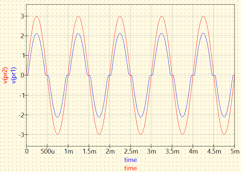
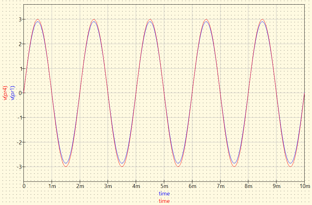
Why this is an amplifier if output’s amplitude is almost equal to the input’s? Although voltage gain is unitary, current is amplified, therefore, its a power amplifier.
The following video shows the amplifiers on a protoboard.
